0.150 → 0.140 mm
112 segments adjusted after impedance, mesh and solder-mask comparisons.
Explore signal resultsLoading saved board and simulation data…
Choose a layer or highlight a net.
Scroll to zoom. Drag to pan.
112 segments adjusted after impedance, mesh and solder-mask comparisons.
Explore signal results106 eligible top-layer segments widened after clearance screening.
Explore power resultsThe selected width balances the two tested solder-mask profiles. At 2.5 GHz the models predict 87.3–94.5 Ω. Fabricator confirmation is needed to set production geometry.
Finite-thickness PEC copper, lossless dielectrics and an ideal adjacent ground plane. Fixtures are included. These local comparisons do not establish whole-channel loss, eye margin or complete rail performance.
| Run | Width | Solver cells | Timesteps | Final energy |
|---|
0.010 mm · relative permittivity 3.5
Dielectric loss and the manufactured mask profile remain unknown. Zero loss tangents are explicit placeholders in the saved stackup.
Only the original Altium Board6/Data metadata was read for this stack. Original route geometry was not imported.
Footprints, pad placement, nets and fixed drawings were preserved. The openEMS adjustment changed only the documented trace widths, stackup and project rules. No new copper, drill, edge or thermal findings were added.
The 199-item capped mask-bridge sample changed by 19 added and 19 removed pad-pair warnings on unchanged footprints.
Resolve retained DRC findings; confirm stackup and mask geometry; verify schematic/net mapping; complete DDR, PCIe and other channel checks; and analyze the entire power system using real loads, component models and thermal/current limits.
112 filled/capped vias require suitable fabrication capability.
| Category | Reported items | Sample scope |
|---|
Counts describe KiCad's reported findings, including capped categories; they are not full violation totals. Download the full DRC record.
All 14 retained runs reached the −50 dB energy criterion. Deep reflection minima remain mesh-sensitive.
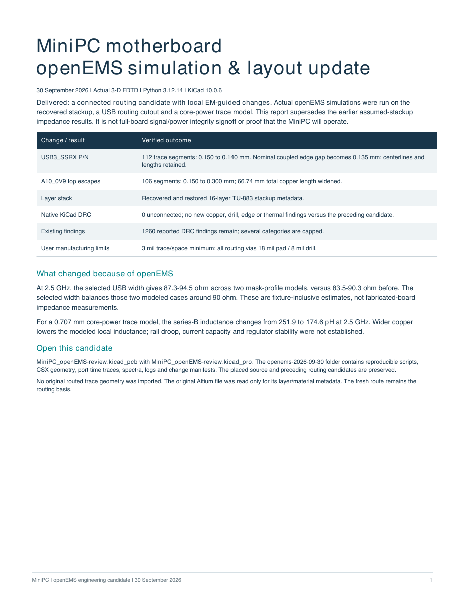
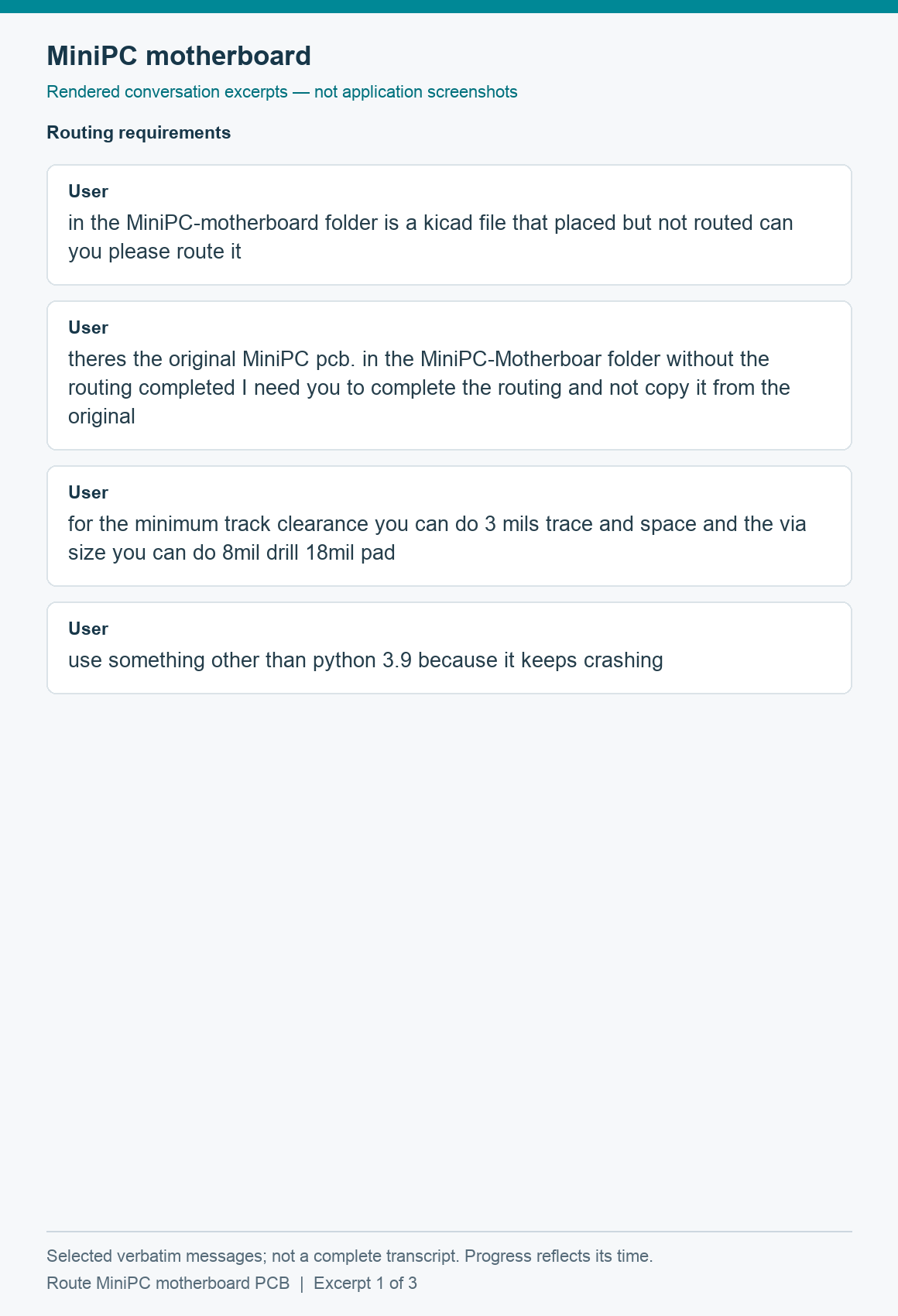
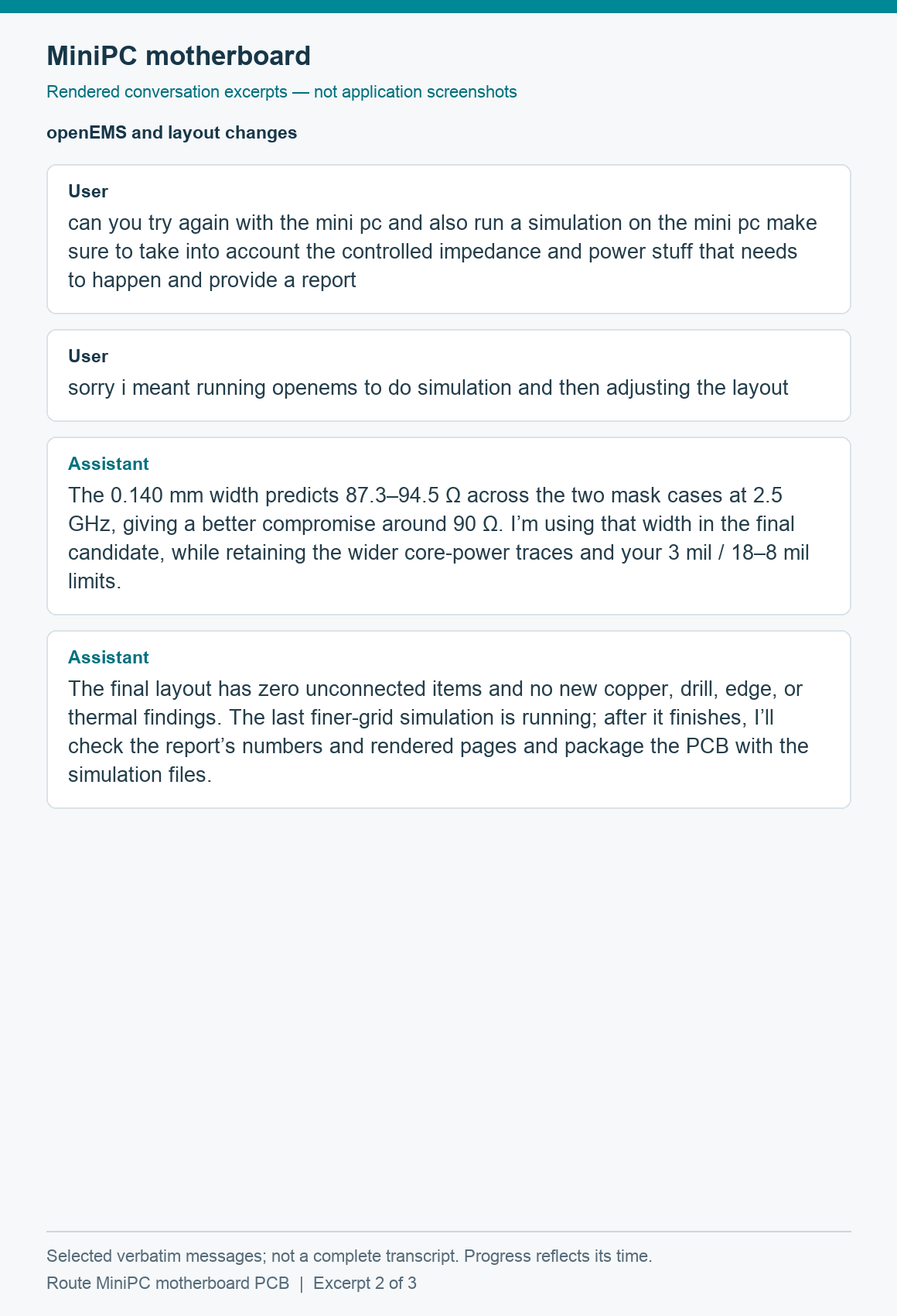
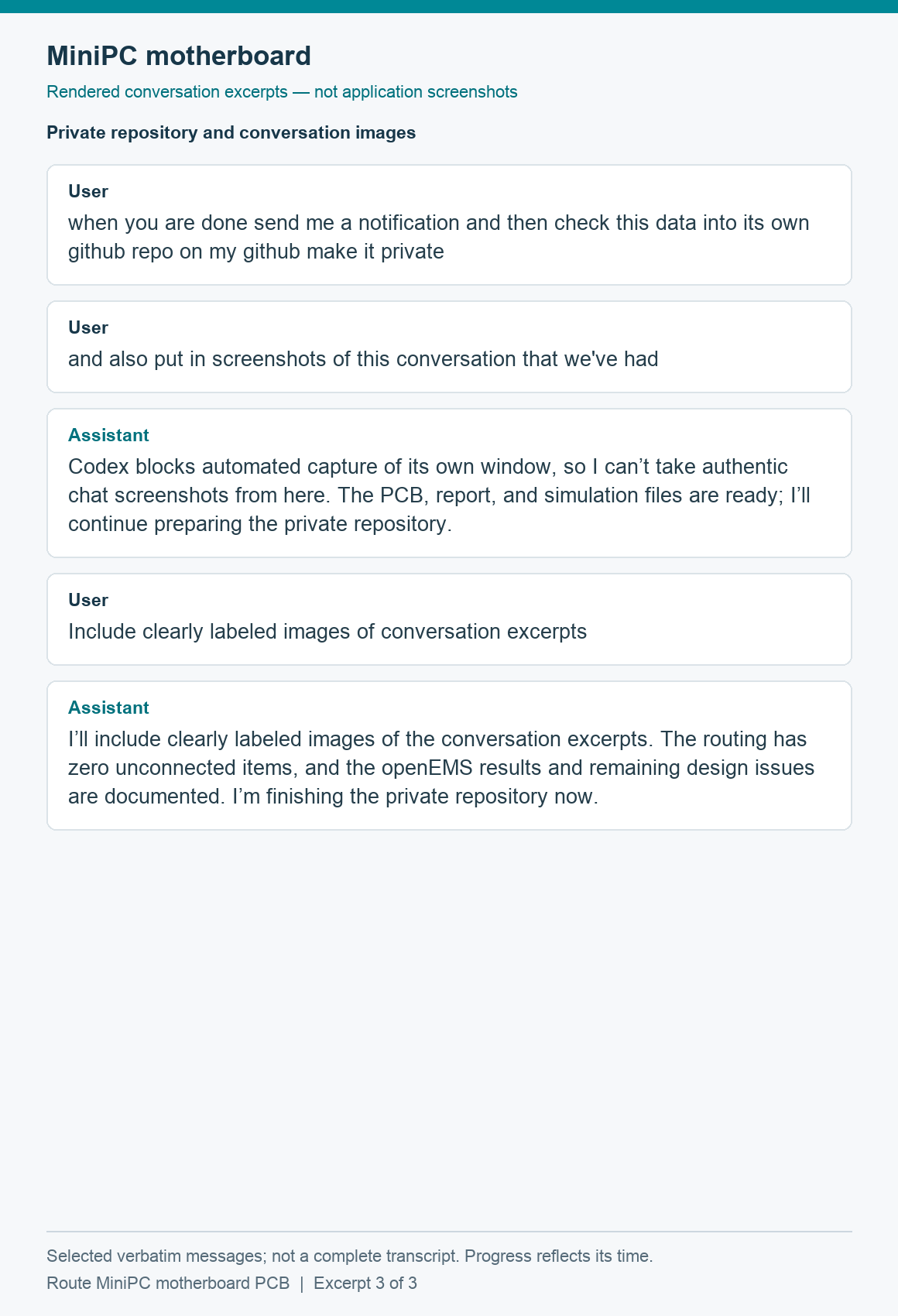
The page images above are rendered from the delivered PDF. The PDF is the canonical report.
Configured 3 mil track/space and 18/8 mil vias. Switched to Python 3.12 and native KiCad checks. Retained placement and generated independent routing.
Rerouted and length-matched the USB receive pair on the top layer. Added 75 ground-return vias in the preceding engineering candidate.
Built the official solver, recovered source layer metadata, compared mask and mesh cases, and retained 14 valid runs. Applied 0.140 mm USB and 0.300 mm power widths.
Packaged the board, report, raw evidence and work records. Prepared this public example review with personal paths and private resource links removed.
Clearly labeled, user-approved images of selected verbatim messages. These are rendered excerpts, not application screenshots or a complete transcript. Progress messages reflect their time. These excerpts predate the user's later approval to publish this example design publicly.
The saved routing candidate, source and preceding board, schematic hierarchy, 14 retained simulations, report, geometry checks and reproduction scripts.
Download final KiCad candidateThe seven bundles below contain the design, accepted simulation runs, raw probes, geometry, reproduction code and checks. Earlier routing checkpoints and rejected experiments are retained in the owner's work archive. The latest report governs the results.
Installed runtimes, dependency caches and original routed Altium geometry are excluded.
e1e56b13565ad465e78f9d0299741d4061a4c4b8146b64bbc53aa9c314169043